Battery formation and test equipment

High‑Precision Battery Formation Solutions

Scalable power solutions for battery formation equipment, delivering ultra‑accurate charge/discharge control, high efficiency, and energy recovery to accelerate EV and energy storage manufacturing.

Energy‑Efficient Battery Formation Systems

Battery formation is a critical stage in advanced battery manufacturing, responsible for activating newly assembled cells through precisely controlled charge–discharge cycles to establish the solid electrolyte interphase (SEI) layer. This process determines a battery’s usable capacity, long-term reliability, and safety, while also representing one of the most time- and capital-intensive steps in battery production. Modern battery formation equipment operates as a highly accurate, multi-channel switched-mode power supply (SMPS) platform, capable of delivering and absorbing DC power across thousands of parallel channels. As global demand for electric vehicles (EVs) and energy storage systems (ESS) accelerates, formation systems have become a key production bottleneck, driving the need for higher throughput, tighter electrical control, and dramatically improved energy efficiency.

onsemi's advanced power electronics are reshaping battery formation system architectures. Wide-bandgap (WBG) technologies such as silicon carbide (SiC) and gallium nitride (GaN) enable higher switching frequencies, lower losses, and greater power density, making fast formation, bidirectional energy flow, and modular system design feasible. Regenerative architectures now recycle discharge energy back to other channels or the grid, achieving system efficiencies above 90% and significantly reducing thermal and infrastructure demands. Combined with advanced AC‑DC power factor correction (PFC), isolated DC‑DC stages, and high‑current multi-channel output converters, these innovations allow battery manufacturers to shorten formation time, improve energy utilization, and scale reliably for next-generation gigafactories.

Block Diagrams

Products

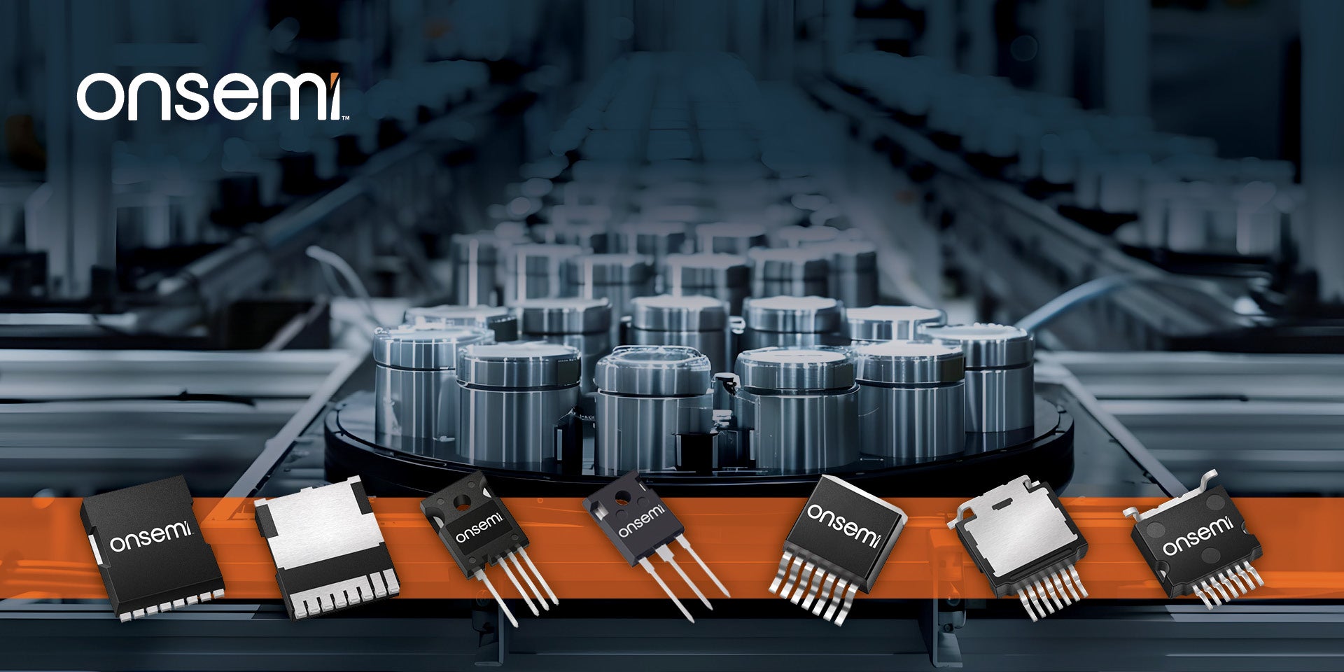
Silicon Carbide (SiC) MOSFETs

Our SiC MOSFETs are designed to be fast and rugged and include system benefits from high efficiency to reduced system size and cost. MOSFETs are metal–oxide–semiconductor field-effect transistors with insulated gates. These silicon carbide MOSFETs have a higher blocking voltage and higher thermal conductivity than silicon MOSFETs, despite having similar design elements. SiC power devices also have a lower state resistance and 10 times the breakdown strength of regular silicon. In general, Systems with SiC MOSFETs have better performance and increased efficiency when compared to MOSFETs made with silicon material.

There are many advantages to choosing SiC MOSFETs over silicon MOSFETs, such as higher switching frequencies. High-temperature development is also not a concern when using SiC MOSFET modules because these devices can operate efficiently even in high heat. Additionally, with SiC MOSFETs, you benefit from a more compact product size because all components (inductors, filters, etc.) are smaller.

Silicon Carbide (SiC) Cascode JFETs
Our high-performance SiC Cascode JFETs utilize a unique cascode configuration, integrating a high-performance SiC fast JFET with a cascode-optimized Si-MOSFET.
Gallium Nitride (GaN) FETs
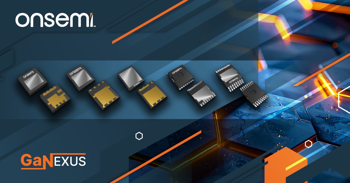
GaNEXUSTM Gallium Nitride (GaN) FETs are enhancement‑mode discrete GaN HEMTs that leverage wide‑bandgap material properties to deliver fast switching, low gate and output charge, and superior efficiency compared to silicon power transistors. These characteristics enable higher operating frequencies, reduced magnetics, and increased power density across low/medium, high and ultra-high voltage power conversion applications.
Gallium Nitride (GaN) Integrated Power
GaNEXUSTM Integrated Power includes GaNEXUS Drive, GaNEXUS Smart, and GaNEXUS Control, where each combines a GaN switch together with potential combination of additional features: gate driver, current sensing, protection, and control, in a single device to simplify design, reduce parasitics, and accelerate time to market.
Low/Medium Voltage MOSFETs
Portfolio of comprehensive range of Low-medium voltage power Mosfets that delivers superior performance and reliability for switching applications. Our cutting-edge PowerTrench® T10 technology delivers industry leading RDS, higher power density, reduced switching losses and better thermal performance.
IGBTs
Insulated Gate Bipolar Transistors (IGBTs) that offer maximum reliability in high performance power conversion applications.
Gate Drivers
GaN, IGBT, FET, MOSFET, H-Bridge MOSFET, and SiC MOSFET inverting and non-inverting drivers ideal for switching applications.
AC-DC Power Conversion
Offline AC-DC controllers and regulators, and power factor and secondary side controllers that enable high active mode efficiency, low standby mode consumption and power factor correction.
DC-DC Power Conversion
A product portfolio for DC-DC charge pumps, controllers, converters, and regulators.
Amplifiers & Comparators
Product portfolio for operational amplifiers (op amp), audio amplifiers, video amplifiers, current sense amplifiers, and comparators.

Documents

Application Notes
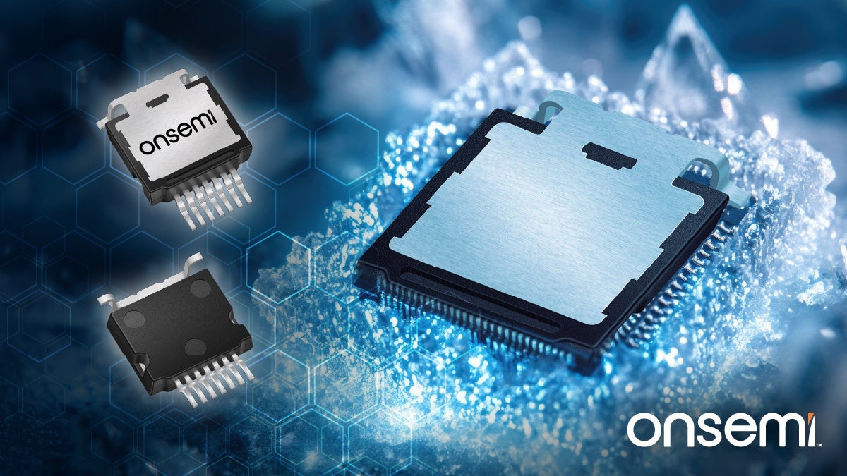
T2PAK: Top‐Side Cooled Package Designed for Automotive and Industrial High Voltage Applications
Application Notes
Using Cascode SiC JFETs in LLC Primary
Application Notes
Design of a Flyback Converter Using Source‐Switched SiC JFET
White Papers
SiC Cascode JFETs: Easing the Transition from Silicon to Silicon Carbide
Application Notes
Paralleling SiC Cascode JFETs
White Papers
3 kW Totem-Pole PFC and Secondary-Side Regulated LLC Power Supply Using SiC MOSFETs
Tutorial
Pairing Gate Drivers to EliteSiC Tutorial
Collateral Brochure
Industrial LDO Selector Guide
Reference Designs
1 kW Universal Input 48 V Output Power Supply Reference Design

Evaluation Boards/Kits

Evaluation Board
NCP1681CCM1KWGEVB
CCM Totem pole PFC 1000 W design with Gate driver integrated GaNFETs
Evaluation Board
NCP1680CRM300WGEVB
CrM Totem pole PFC 300 W design with discrete GaNFETs
Evaluation Board
NCP5183SYNCBUCKGEVB
Variable DC Input, Open Loop Synchronous Buck Evaluation Board
Evaluation Board
NCP51810GAN1GEVB
100V eGaN Half Bridge Gate Driver Evaluation Board
Evaluation Board
NCP-NCV51561D2PAK7LGEVB
NCP/NCV51561 EVB OPN
Evaluation Board
NCP13994MM360GEVB
All-in-One 360 W power supply using NCP1618, NCP13994, NCP4318 and NCP431

Design Resources

Tools and resources for your evaluation process.

Find the Right Product

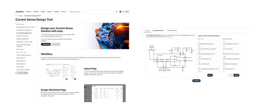
Utilize our PRT+ tool to identify the ideal product for you.

System Solution Guides

Explore tailored components and insights for your application.

Evaluation Boards & Kits

Buy and validate the performance of chosen components.

FAQs

Formation can take 10–20 hours or more per cell and must be performed on every unit with tight current and voltage accuracy. As battery demand scales, this slow, energy‑intensive step limits factory throughput and accounts for a significant share of equipment cost and floor space, especially in high‑volume EV and energy storage manufacturing.

Battery formation equipment functions as a large, multi‑channel switched‑mode power supply platform. Power electronics enable ultra‑precise current and voltage control, high parallelism across thousands of channels, and efficient handling of both charge and discharge energy, which is essential for accuracy, scalability, and energy efficiency in modern formation lines.

Bidirectional architectures recover energy during cell discharge and reuse it within the system or feed it back to the grid. Instead of dissipating discharge energy as heat, regenerative designs dramatically improve system efficiency, reduce cooling requirements, and lower operating costs, enabling round‑the‑clock operation with much higher overall energy utilization.

Wide‑bandgap devices such as SiC and GaN enable higher switching frequencies, lower losses, and higher operating temperatures. This translates into higher power density, improved efficiency, smaller passive components, and reduced cooling requirements, all of which are critical for compact, scalable, and energy‑efficient formation systems.

A typical system includes an AC‑DC front end with power factor correction, an isolated high‑power DC‑DC stage, and multiple low‑voltage bidirectional DC‑DC output channels. Together, these stages enable efficient grid interfacing, galvanic isolation, precise cell‑level control, and energy recovery during discharge.

Worth Your Time

Discover curated articles brimming with innovative insights and industry trends.

Related Videos

Let's keep going – watch these videos for deeper dives and fresh perspectives.

Find Support

Your support sources for product info, knowledge base and FAQ for fast solutions.

Icon for support at onsemi
Support Hub

Explore the various contact options at onsemi support. 

Contact sales at onsemi
Sales Team

Get help with product or design questions by sending us a message or finding Sales Contacts on our Sales Office page.

Icon for community forum at onsemi
Community

Collaborate with engineers, share ideas and access peer-to-peer solutions for your projects.

battery formation