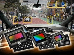
In a highly competitive and fast moving sector, automakers and their suppliers want to add an increasing number of new safety and convenience features to vehicles. But they need scalable solutions to bring them to market across their product ranges from luxury to economy models, in a rapid easy-to-design-in and ultimately cost effective way.
Scalability has value across many device and technology types in the automotive sector. As we see increasing numbers of cameras on vehicles and progress through the levels of autonomy towards the holy grail of driverless cars, sensors and perhaps most pertinently image sensors, are among those parts where areas of commonality across a platform can hold great value to automotive design engineers.
ON Semiconductor’s Hayabusa™ family is the first highly scalable family of automotive image sensors. Featuring the same 3.0 µm backside-illuminated (BSI) pixel architecture across devices at different resolutions means that applications from front view advanced driver assistance systems to rear view cameras, surround view and automated parking systems can enjoy the significant benefits of common platform features.
The performance requirements for image sensors used in automotive applications are stringent both in terms of the environment in which they must operate and the scene situations they have to cope with. Space and weight constraints, vibration and extremes of ambient temperature are already well-known to suppliers of components or systems to automotive applications and the modern CMOS image sensor is well-suited to these demands.
The scenes that image sensors have to deal with can see rapid changes from light to dark and vice versa - when entering or exiting a road tunnel during daylight hours for example. The Hayabusa family’s pixel architecture features Super-Exposure technology which increases the dynamic range or scene content that is captured in a single frame. This also results in being able to offer High Dynamic Range (HDR) output simultaneously with LED flicker mitigation (LFM) as a common feature across the platform. With the increasing popularity of pulsed LED lighting on vehicles and road signs, LFM is essential to mitigate the appearance of flicker from such light sources, which human eyes cannot perceive, while preserving the scene detail of HDR output.
Image sensors such as the Hayabusa family used in combination with other sensing technologies such as LiDAR and radar will be pivotal in ensuring the realization of safe and effective ADAS and ultimately, fully autonomous driving. The engineering design challenges of rolling out image sensing solutions across applications and on various vehicle model ranges can be significant, especially in the face of time and cost pressures in addition to the unique working environment that the automotive market presents. Because of this, commonality and scalability across a high-performance image sensor platform is an extremely welcome reality for automakers and their system suppliers.
ON Semiconductor’s scalable Hayabusa family with its common pixel architecture is expanding to offer three resolutions: 3.1 Megapixel (MP) with a unique 8:3 wide aspect ratio for wide field-of-view applications, the 1.3 MP that comes in a compact 8mm by 7mm automotive qualified packagemaking it ideal for megapixel-based rear view cameras, surround view systems and automated parking systems where space constraints are a factor, and the existing, highly versatile, high-performance 2.6 MP device.
