As the need and desire for electric vehicles (EVs) continue to accelerate, the DC fast charging (DCFC) market thrives, and the demand for fast-charging infrastructure continues to increase. Growth projections range from 20% to 30% CAGR for the next five years. Suppose you are an application, product, or design engineer in the power electronics field; sooner or later, you could take part in the design of such a novel charging system.
A fundamental question might arise here, especially if it is the first time you have faced such a challenge. How and where should I begin? What are the critical design considerations, and how should I address them? onsemi helps designers overcome these challenges, as we will demonstrate by developing a 25 kW DC fast charger based on SiC power integrated modules (PIM).
Developing this type of high-power battery charger requires a diverse skill set. An expert onsemi team led the project coordination on this design, undertook all the hardware development activities, and developed the firmware and software. The team brought years-long development experience in control and algorithms for power converters and motor drives.
We will walk through the development process of the DC charger, addressing different topics along the way. We will highlight the key challenges, trade-offs, and compromises and show how to design, build and validate such a system from scratch. The design journey is not straightforward; the best way to move forward is to get running and iterate fast.
DC Fast Charger − What Are We Building?
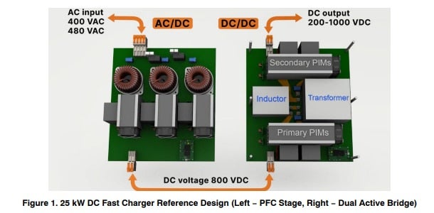
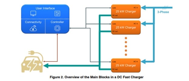
In the e-mobility ecosystem, direct-current (DC) chargers provide “fast” and “ultrafast” charging capabilities, in contrast with slower alternating current (ac) chargers. In essence, EV chargers convert the AC power from the grid into DC power suitable for delivery into the batteries of the EVs. The power conversion in DC charging is handled outside the EV (“off−board”) and then delivered to the vehicle with power levels ranging from below 50 kW to greater than 350 kW (with even higher levels in development). Higher-power DC chargers are typically built modularly, stacking power blocks of 15 to 75 kW (and above) in a single cabinet (Figure 1). In general, output voltages of DC chargers range from 150 V to above 1000 V, covering both the 400 V and 800 V standard EV battery levels, and may be optimized for the higher or lower voltage end.
The architecture of such power blocks is as follows: an AC-DC boost converter with power factor correction (PFC) at the front end, followed by a DC-DC stage that provides isolation between the grid and the load (battery of the EV) and regulates the voltage and current at the output (Figure 2). The system may also be bidirectional (particularly at lower power), and thus the topology and design should account for it.
The onsemi team is developing a 25 kW DC charger with bidirectional capability. The system shall cover a wide output voltage range, have the ability to charge EVs with both 400 V and 800 V batteries, and be optimized for the higher voltage level. The input voltage is rated for EU 400 Vac and US 480 Vac three-phase grids. The power stage shall deliver 25 kW over the 500 V to 1000 V voltage range. Below 500 V, the output current will be limited to 50 A, derating the power in alignment with profiles of DC charging standards such as CCS or CHAdeMO (Figure 3).
Regarding communication ports, the board will provision isolated CAN, USB, and UART infrastructure for external interfaces (between power blocks, charger system controller, vehicle, service, and maintenance). Overall, the design will follow guidelines from the IEC-61851-1 and IEC-61851-23 standards for EV charging. The table below summarizes the system requirements.
The Development Process
Our team follows the logic of hardware development processes of power conversion. The work starts with the definition of the actual DC charger power stage based on the requirements for the application. Summarized in the table in our case, these are per the market’s needs and follow the guidelines of IE-68515. These requirements help the team understand their target. The first feasibility studies help validate the initial requirements and assumptions, integrated as part of the system design that encompasses (in this project’s scope) hardware, software, thermal management and mechanical design, prototyping, and validation. All the essential system variables, most critical compromises, and trade-offs for the solution happen during the feasibility studies. Multiple iterations carry out these tasks and sub-designs where outputs and assumptions from one part feed back to another. Two of the main design activities that provide significant results to move forward are:
Power simulations are crucial to confirm the assumptions on working voltage and currents, losses, cooling requirements, selection of power, and passive components, among others. Once an implementation plan is ready, control simulations, including the power parameters, are carried out to confirm the effective execution of the control loops with the power design. Proving the design with the power and the control simulations greenlights the schematics drawing, PCB layout, and prototype manufacturing. After board development, we carried out hardware bring-up, functionality testing, and system characterization. Please refer to Developing a 25 kW EV DC charger from scratch entails more than that; the most valuable takeaways will come as we solve the challenges and issues along the way.
(*Please watch the four-webinar series of “Designing Silicon Carbide (SiC) based DC Fast Charging System” for more details.)
What Is Coming?
In subsequent parts of this reference design series, we will look closely at some design and validation stages. Continue to read the reference design series!
If you have a question about a 25 kW SiC−Based Fast DC Charger or this reference design series, please get in touch with Technical Support.
Karol Rendek
Karol Rendek is an Applications Manager at the Systems Engineering Center at onsemi. Karol joined onsemi in 2020.
Previously, he spent nine years working as a hardware engineer, system engineer, and project manager in the development of embedded systems, Class D amplifiers, rolling stock control and safety systems, and industrial electric vehicle chargers.
Karol has a master’s degree and Ph.D. in Microelectronics from the Slovak University of Technology in Bratislava. He spent three years during his Ph.D. study focusing on low-frequency noise analysis of GaN HEMT transistors.
Stefan Kosterec
Stefan Kosterec is an Application Engineer at the Systems Engineering Center at onsemi. Stefan joined the company in 2013. Stefan has a master’s degree in Applied informatics from the Faculty of Materials Science and Technology of Slovak Technical University Trnava.
Previously, he worked for eight years at Siemens PSE as ASIC/FPGA designer, developing digital solutions targeted at various areas, such as communications, power conversion, and motor control. He also spent two years at Vacuumschmelze, acting as an inductive components designer, and took the role of product integrity engineer at Emerson Energy Systems, where he was responsible for telecom power systems verification.


