Many applications in the electronics industry ranging from sensor-based designs to power amplifiers are periodically faced with the requirement to generate a negative voltage rail. Although many transformer-based designs, charge pumps and other methods have been used to meet this specific requirement, the inverting buck-boost topology stands out as simple to design and can save on power and board space at the same time.
Power budgets in many applications are already stretched, and PCB real estate is often limited due to the clashing requirements of customer pressure to shrink solution size at the same time as wanting high levels of functionality incorporated in many new products. Power devices that use an inverting buck-boost topology can provide a solution, and therefore be extremely valuable to systems designers.
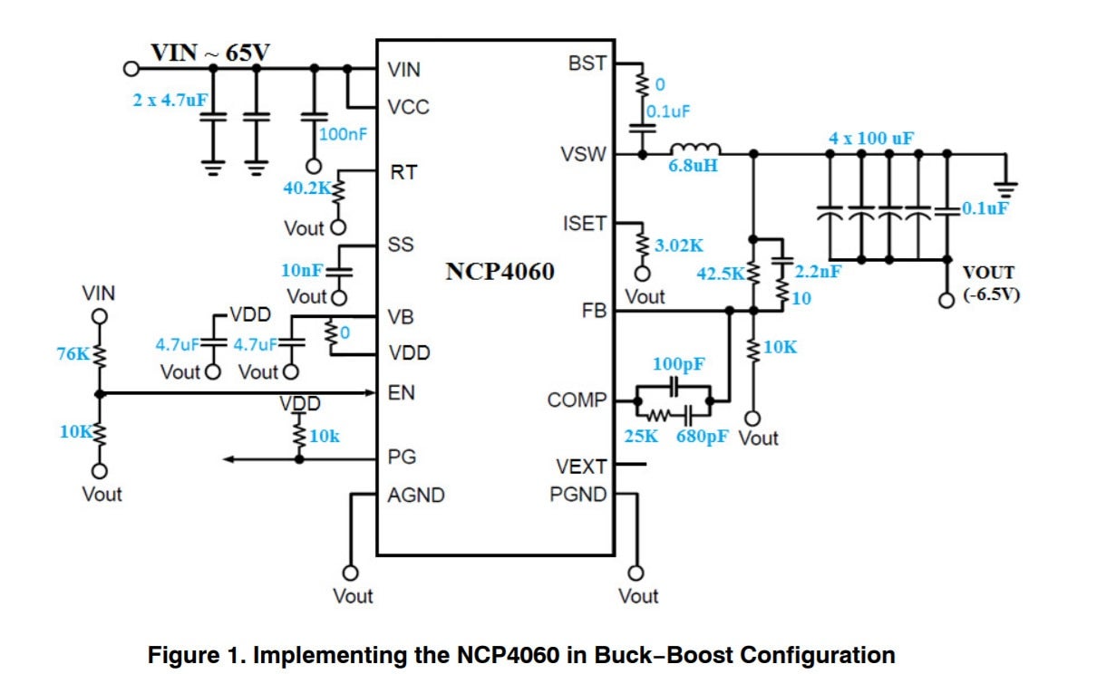
A Buck regulator can be reconfigured to generate a negative output voltage from a positive input voltage using the inverting buck-boost topology. Unlike a buck regulator, the inverting buck-boost transfers energy to the output through the output diode during the ‘off’ time. For this reason, users must keep in mind that the average output current is always less than the average inductor current. Designers must also be mindful that the device is no longer referenced to Gnd but to the negative output voltage, which makes the effective input voltage across the device VIN + |VOut|.
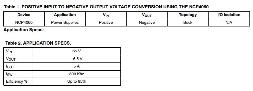
Telecommunications vendors tend to adopt a two-stage design to generate a negative voltage rail for the GaN PA driver. The first stage steps down the input voltage (48-65V typically) to 12V, followed by a second stage that generates -6.5V. By using a device such as ON Semiconductor’s NCP4060A, designers can consolidate this into one stage that takes the high input voltage and converts it down to a negative output voltage while sustaining good efficiency and offering a solution for space-constrained applications.
There are a number of important factors and challenges to consider when adopting buck-boost topologies. ON Semiconductor’s NCP4060A is an 80V synchronous buck regulator with integrated power FETs that can accommodate up to 6A DC loads. It is a good example of a device that provides the flexibility to down convert from high input voltages to negative output voltages just by exchanging Vout with Gnd on a buck.
The implementation steps to reconfigure a buck IC to an inverting buck-boost circuit to generate a negative voltage from a positive input are relatively straight forward however, there are a few design tips worth noting and following to stress the fundamental differences between a Buck regulator and the Inverting Buck-Boost.
More information about these can be found in the High Voltage Inverting Buck Reduces Complexity and Board Space App Note.


