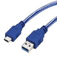
USB has evolved from a data interface capable of supplying limited power, to a primary provider of power with a data interface. The latest USB 3.x protocol supports power flow at a much higher level. With a default 5V voltage, the USB-C port is capable of negotiating with a plugged-in device to raise the port voltage up to 20V.
A unique challenge in the new power delivery requirement is how to use a 4.5V-32V input voltage to provide a 5V-20V DC bus. A 4-switch buck-boost converter is a suitable topology to provide the buck or boost power conversion, because it provides a wide voltage conversion range, positive polarity, high efficiency and a small form factor solution size that designers and customers require. ON Semiconductor’s NCP81239 4-Switch Buck Boost Controller for USB Power Delivery and USB-C Applications can drive 4 switches, allowing the converter to buck or boost and support the consumer to meet the USB Power Delivery (PD) specifications which is suitable for all USB PD applications such as PC/Laptop, power bank, and docking station.
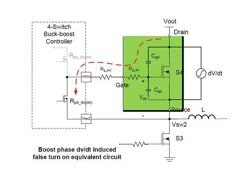
In synchronous buck converters, there is a well-known phenomenon called “low side false turn-on,” or “dv/dt induced turn on”, which is the culprit for shoot through that potentially damage the switch and reduce the reliability of the entire converter.
Then the problem is doubled in a 4-switch buck-boost converter because it has two phases – a buck and a boost. Errors are made when designers simply copy the circuit parameters of a buck converter directly to the boost phase of a 4-switch buck-boost converter. As this topology gains more popularity in applications, the dv/dt induced turn on issue is becoming more important to understand.
Dv/dt induced turn on in a 4-switch buck-boost converter is caused by a rapidly rising drain-source voltage at the synchronous rectifying MOSFET in both the buck phase and boost phase. As a result, the overall system efficiency deteriorates because of the undesired shoot through currents flowing in either phase leg. Several economical circuit solutions are available to the power supply designers, these include: minimizing the rectifying switch’s turn off gate drive resistance, increasing the active switch’s turn on gate drive resistance, or adding RC snubber circuit to the switching nodes. Choosing MOSFETs with small Qgd/Qgs(th) ratio and high threshold voltage can also decrease dv/dt induced false turn on possibility.
Learn more details by checking Gate Driver Design Considerations for 4-Switch Buck-Boost Converters to find out more details.

