Delivering the levels of power needed to safely and efficiently enable faster electric vehicle (EV) charging and support accelerated adoption is not trivial. With further significant improvement in silicon-based switching devices becoming ever more challenging, leading semiconductor device manufacturers such as ON Semiconductor are working with new materials to provide solutions with the performance needed for rapid EV charging. So-called wide bandgap (WBG) materials including gallium nitride (GaN) and silicon carbide (SiC) both present significant benefits for power designs related to EV charging.
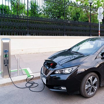
EVs and their similar counterpart Hybrid Electric Vehicles (HEV), are becoming a more common sight on our roads, especially in urban areas where EV charging stations are increasingly common. While there is a significant amount of pressure from environmental lobbies and governments to adopt these new vehicles, many would say that the uptake has been disappointing, so far.
Common obstacles related to EVs
Range anxiety – the concern that the driver will become stuck with no charge – has been accredited as a reason for the slow sales, but with more charging points being added, this is now diminishing – especially for shorter journeys and regular commutes in more urban areas. In many cases, vehicles can be charged overnight at home, ready for the next day’s commute or travel needs. The rate of increase in the provision of charging points varies globally with some countries such as China where pollution has resulted in very specific targets advancing more quickly.
However, for journeys that exceed the capacity of the vehicle’s battery, there is another issue, even if charging stations are available. The battery charging process is simply too long, meaning that in some cases it would be hard to complete a 300-mile journey within a day. This inconvenience is another factor that is slowing the adoption of EVs.
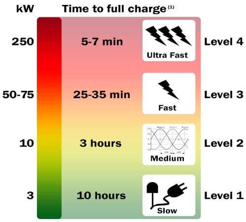
Currently, there are several tiers of charging available. The most basic (Level 1) involves plugging the vehicle into a normal outlet and waiting. Capable of delivering up to 3 kW of AC power a full charge can take up to ten hours which is viable for overnight charging, but little else. Level 2 can also be used in the home environment as it delivers up to 10 kW from three-phase power, reducing a full charge to around three hours which is much more viable for charging while performing an activity such as attending a meeting, shopping or eating out.
However, there are two main drawbacks to AC-based charging; first, it requires several hours at best so it is not convenient mid-journey, especially when replenishing a gasoline fuelled vehicle takes just a few minutes. Also, as the vehicle battery requires DC to charge an on-board AC/DC converter is required which adds weight to the vehicle and reduces efficiency, thereby reducing the range.
Commercial charging stations are higher power and tend to primarily use DC to feed power directly to the battery, removing the weight and efficiency loss of the AC/DC converter. Level 3 charging stations are able to deliver up to 75 kW of power which can recharge a fully depleted battery in around 30 minutes. While not as convenient as refueling a gasoline car, this is now reaching a level where it would be acceptable during a long journey.
The highest power level is provided by Level 4, around 250 kW which can provide enough charge to replenish an empty battery in around six minutes. As the transition to EVs continues, provided sufficient numbers of these charging stations are deployed, then the ‘charging convenience’ objection to EVs will be removed.
How ON Semiconductor is providing solutions to these obstacles
Devices based on WBG materials being developed and introduced by ON Semiconductor can deliver the performance and characteristics that design engineers in this space need. Both SiC and GaN have lower static losses through lower on-resistance (RDS(ON)) and also a lower level of gate charge (Qg) which reduces the switching losses. As a result, WBG-based power designs can operate at higher frequencies, reducing the size of magnetic components and the overall size of the solution.
WBG also allows the values of capacitors and inductors to be reduced by around 75%. This reduces passive and magnetic component costs significantly, offsetting the higher cost of the switching devices. As a result, high-performance, highly-efficient WBG-based power designs have now reached a point where they are lower cost (and substantially better performance) than the equivalent silicon-based design.
ON Semiconductor supplies all of the components needed to build a Vienna rectifier-based charging solution. We offer an extensive 1200V SiC Schottky diodes portfolio, such as the 1200V, 30 A FFSH30120A which has no reverse recovery current and temperature independent switching characteristics. In addition we offer a wide variety of advanced SiC MOSFETs such as the NVHL080N120SC1 or NVHL020N120SC1 which have an on-resistance (RDS(ON)) ranging from 80mOhm down to 20mOhm with low gate charge and capacitance that reduce EMI and permit faster operation.
SiC devices require advanced gate drivers to ensure optimum performance and the NCP51705 ensures the lowest possible conduction losses by delivering the maximum permissible gate voltage to the SiC MOSFET.
Learn more about EV charging stations today, as well as how utilizing WBG in EV charging stations can benefit your designs!


