As we automate our modern world, sensing is rising in importance in all areas. Many types of sensors exist, from the simplest that monitor a single parameter (such as light or temperature) to more sophisticated devices such as image sensors capable of recording an entire scene at incredible frame rates for analysis.
Image sensors continue to rise in popularity and are used in many applications ranging from the obvious to the unthinkable. In the industrial sphere, they can monitor security, check on a process, inspect finished goods or work-in-progress (WiP), check any flat panel display, and even shoot your favorite Hollywood movie. However, unlike employees, image sensors never miss anything and can work 24/7/365.
The Design Challenge
Designing a camera system can be challenging, and, in industrial applications, there can be additional challenges due to the environment (temperature, humidity, dirt, electrical spikes)—a very long list. However, the most fundamental decision is usually the sensing element, the image sensor, which can make or break a design.
Sensor resolution is one of the critical decisions to make—the captured image or video stream has to be detailed and fast enough so that the person (or software) monitoring it can pick out the detail at the required speed. However, adding resolution while running the sensor at a rate the downstream electronics cannot handle will increase the cost of the sensor and require more bandwidth for transmission and storage capacity, further increasing costs. Therefore, it is essential that the sensor specified is adequate for the task but not over-specified.
Resolution is also associated with power consumption, and this is less of an issue in many cases where the system is mains-powered. But for battery-powered equipment—such as drones, portable testers, IoT devices, or even the automatic guided vehicles (AGVs) that are becoming more common in factories and warehouses—an over-specified sensor can significantly reduce the useful working time between charges. Furthermore, too much power dissipation results in excessive heat dissipation, which eventually creates noise affecting the overall image quality.
In the many applications within a modern industrial setting, cameras perform different tasks, each requiring different resolutions. For example, a simple detection application could use low-resolution cameras, whereas applications requiring the inspection of detailed features would deploy high-resolution cameras.
While this approach avoids the pitfalls of over-specifying the sensor, it does require different sensors for each resolution. Unfortunately, a different design is required for each sensor in many cases, thereby multiplying the design task (and time) significantly. The ability to benefit from economies of scale diminishes even when the designs are complete, as each uses different components.
The convenience and value of image sensors make them popular, leading to many companies adopting the technology for the first time. However, the learning curve can be very steep—and designs can even be tricky for experienced designers.
The Family Approach Brings Benefits
Despite the need for a range of cameras at different resolutions with different feature sets, designers would prefer to complete just one design in the ‘ideal world.’ However, that seems impossible due to the need for different sensors to optimize each camera to a specific application.
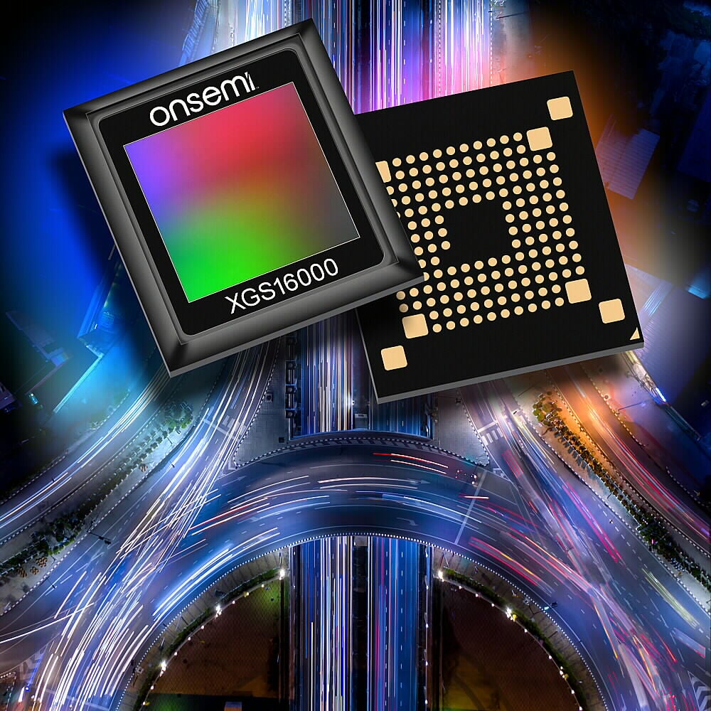
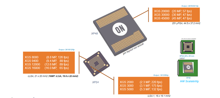
However, with our PYTHON and XGS series of advanced image sensors, onsemi has taken a ‘family’ approach. While seven different XGS sensors offer a range of resolutions from 2.3 megapixels (MP) to 45 MP, all devices have a common footprint compatible with the industry-standard 29 mm x 29 mm layout. At the higher resolutions, the four XGS devices for the 20 MP to 45 MP range also share a common, albeit different, footprint. A similar approach was chosen for the PYTHON family, offering a resolution starting at 1.3 MP and going up as high as 26.2 MP.
A single camera hardware design up to 45 MP (and another for higher resolutions) with known performance goes a long way to addressing a designer’s wish for a single design, significantly reducing design time and risk while allowing access to economies of scale in manufacturing. Additionally, intellectual property (IP) such as firmware can be re-used throughout the series of cameras, and if a hardware firmware update is needed, it only has to be done once, reducing design maintenance costs.
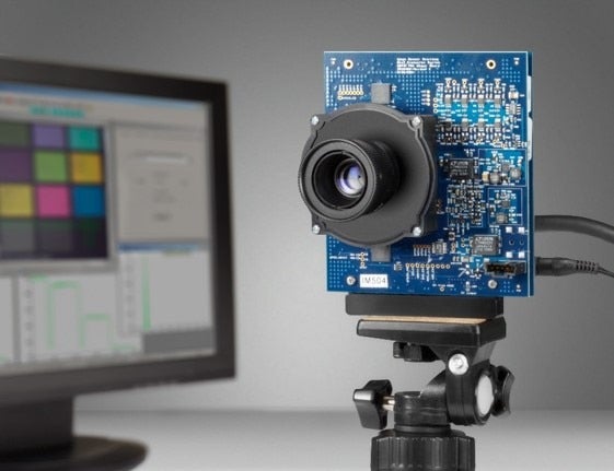
onsemi provides several development tools, including a demo kit with a hardware platform and DevSuite software for sensor evaluation to support designers new to image sensing. Also available is the X-Celerator platform with FPGA code that interfaces directly with Altera® and Xilinx® and the X-Cube reference design that uses a Lattice FPGA for HiSPi-to-MIPI conversion. X-Cube also uses the DevSuite software for image capture, processing, and analysis.
Learn more about onsemi industrial imaging solutions.