Previously in our blog, we talked about “Power Supply Rejection Ratio (PSRR) Real-World Perspective - Part IV” describing PSRR parameter on examples. Continuing our blog series, this blog will focus on the meaning of “dropout” and discuss ON Semiconductor’s product and solution offerings for LDOs (Low DropOut Regulator) in regards to low dropout and very low dropout values. Do you need LDOs with low dropout for your applications? We will describe what dropout means, how it is measured and the difference between LDO with a normal dropout and very low dropout.
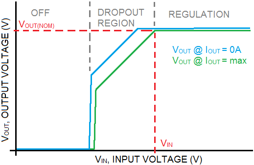
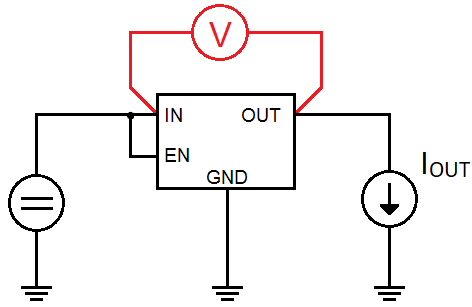
It´s necessary to have higher headroom VIN – VOUT than the value of the dropout parameter of LDO. Dropout is one of the most critical parameters for the LDO to function correctly. Dropout is the difference of VDO = VIN – VOUT,NOM which LDO needs to regulate properly. VOUT,NOM is the nominal value of output voltage which is at the output when LDO is in regulation. The dropout value is usually measured when VOUT is lower (about 3%) or 100mV than the nominal value. It´s easy to measure the value when VOUT falls, for example about 100mV. The Dropout parameter is usually measured for nominal output current because dropout is measured when VOUT falls, roughly 3% below VOUT,NOM. Thus, the output has to be connected to the current source in sink mode, for example, active load to sink constant current. In the case of resistance connected to the output, load output current would decrease and the measurement would be invalid, see the below image.
LDO should have a voltage difference between VIN and VOUT with a higher dropout value of VDO to achieve good dynamic performance.
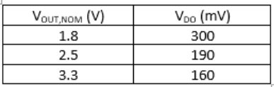
Most of LDOs have pass device MOSFET P-Channel (PMOS), this is a bit of a disadvantage for lower output voltages. Dropout VDO of LDO with PMOS pass device increases when nominal output voltage VOUT,NOM is lower. As an example, look at the following table and let’s say we are using NCP161. You can see 1.8V option has a much higher dropout value than 3.3V option.
PMOS device LDOs have disadvantages since they have pretty high minimal input voltage VIN,MIN. NCP110 is also a PMOS device LDO, it is ultra-low VIN. It has VIN,MIN = 1.1 V. NCP110’s lowest output voltage option 0.6V has a dropout value of 500 mV.
If there is a request for a very low dropout or output voltage option close to 0V it´s possible to use Bias Rail LDO. This kind of LDO has pass device MOSFET N-Channel (NMOS) and it needs to connect auxiliary supply VBIAS which has to be higher, about 1 V – 2 V than VOUT to achieve very low dropout. Bias Rail LDO has the same structure as conventional LDO but the supply for internal blocks (everything but pass device) is not connected to VIN. It is separated as a second supply. A few examples of these devices are NCP130, NCP134, NCP137, and NCP139. LDOs with NMOS pass device, have almost independent dropout values of output voltage when compared to a LDOs with PMOS pass device.
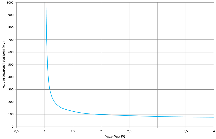
These devices have dropout values of VDO in the range of 40 mV ~ 150 mV at nominal output current. But it´s necessary to have VBIAS voltage connected as mentioned otherwise dropout is much higher, due to Volt units. In the following picture, you can see what happens to dropout of NCP134 when the difference VBIAS - VOUT goes down, thus the VBIAS voltage is not high enough.
It is also possible to have LDO with pass device NMOS but without VBIAS supply. There is a charge pump device used to supply internal blocks. The charge pump device creates double the higher internal VBIAS voltage from VIN supply.
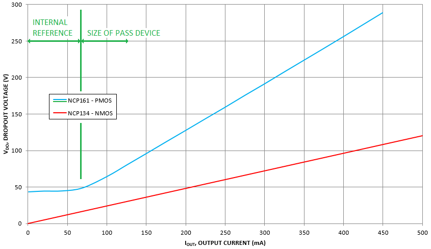
In figure 4, you can see the difference between the dropout of LDO with PMOS pass device and a LDO with NMOS pass device. A LDO with PMOS pass device usually has a non-zero dropout value at zero output current. This part of LDO dropout is the dropout of the internal voltage reference. The second part is a dropout set by the size of a pass device. LDO with NMOS pass device has internal reference supplied from VBIAS voltage. So it does not have the first part. Dropout of LDO with NMOS pass device is set only by the size of a pass device.
Be sure to subscribe to our blog and follow us on social media to receive the latest updates on our technologies, solutions and company news!
Twitter | Facebook | LinkedIn | Instagram | YouTube