There are many reasons why integration is a good thing, but every increase in integration normally comes with demand for more power. Point of Load (POL) regulators do a great job of responsibly delivering that power where it’s needed and at the right level, however they also have their challenges.
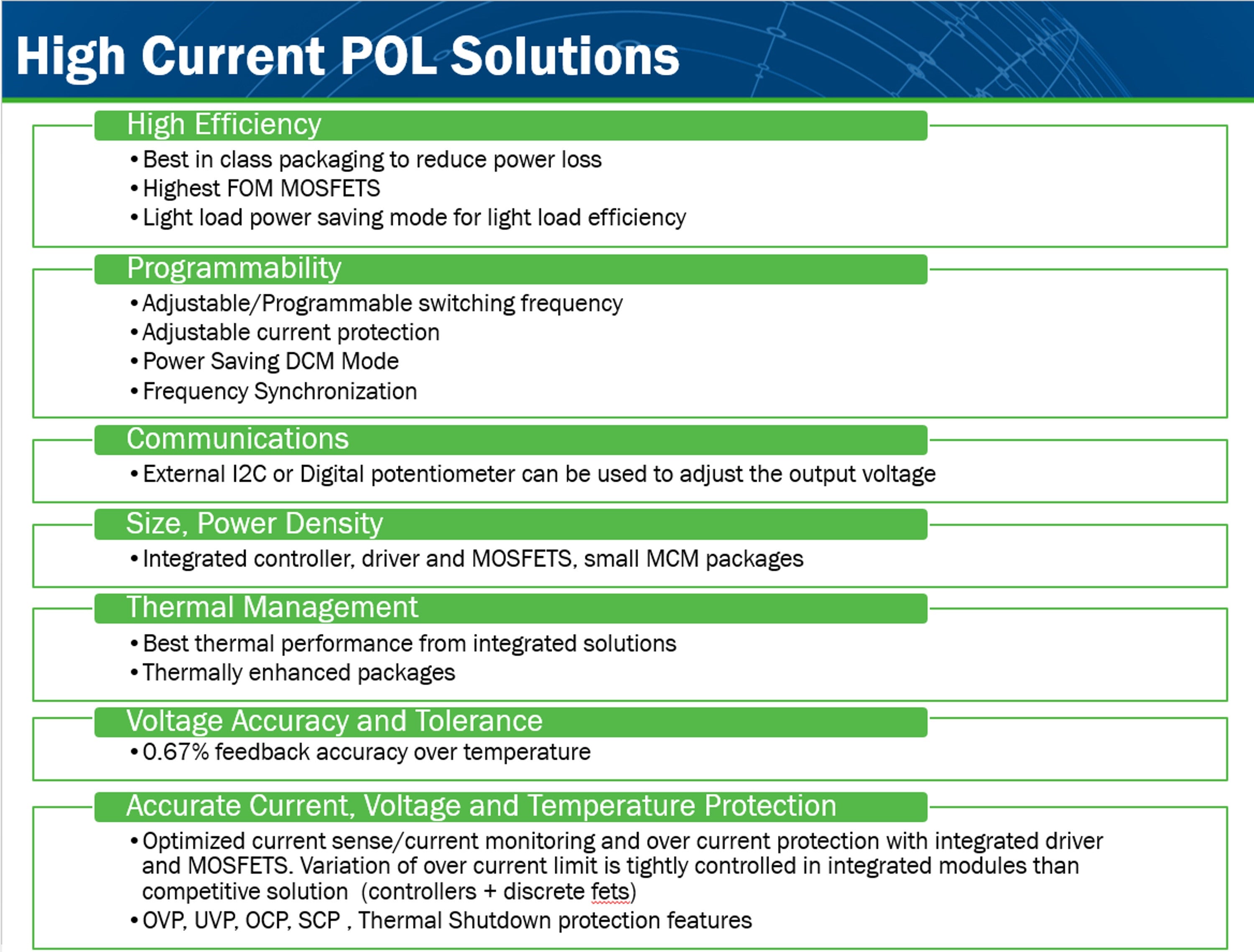
These include high efficiency with the right power density, of course, but extend to programmability and flexibility, with fast transient response, tight tolerances and accuracy. All this, has to be wrapped up in a solution that has reliable current and voltage protection with excellent thermal management.
Power conversion and regulation needs to reach new levels of efficiency in order to deliver more power without burning through the thermal budget. At the same time, manufacturers want higher levels of integration and smaller PCB footprints, so is it possible to meet all these requirements?
High Current POL applications do come with a long list of challenges, but the FAN6500XX family of products has been designed to handle them. The FAN65004B/5A/8B family can deliver up to 100W of power with high efficiency of 95%, delivering excellent thermal performance with a mere 29°C rise in temperature in a small 6x6mm PQFN35 package. Moreover, the FAN65 family has a power saving mode for improved efficiency under light load conditions.
The FAN6500xx is a multi-chip module packed with all the required active components needed to produce an intermediate-bus for POL applications, including a synchronous buck PWM controller, drivers, and two MOSFETs (High-side and Low-side). This high level of integration reduces the need for multiple external components, while allowing optimal output filter L and C components to be used. Optimized package design, strong analog expertise, and exceptional Figure-of-Merit (FOM) MOSFETS make the FAN6500XX a best-in-class solution.
A big advantage of developing all the components in a multichip solution is that it allows for design optimization between the Gate driver and the MOSFETs. FAN6500XX uses ON Semiconductor’s PowerTrench® MOSFET technology. This shield gate technology delivers lower switch node ringing and reduced risk of shoot-through or cross –conduction. Reliability is also improved as the modular approach means there is now only a single point of failure in the power supply design.
This wide Vin (65V) product family is differentiated by output currents of 6A, 8A or 10A. Pin-compatibility and scalability between all parts ensures that OEMs can choose the most optimum device for their application even after the PCB design has been finalized. The fixed frequency voltage mode PWM control topology allows for easy compensation, low output ripple and low EMI. The FAN6500XX offers optimized performance for both high (Suffix “A”) and low (Suffix “B”) duty cycle applications.
A higher power requirement is addressed by a programmable and synchronizable switching frequency (100Khz – 1MHz) feature that ensures low input ripple when multiple FAN6500XX devices are used in parallel.
The FAN6500XX devices support a wide input voltage range from 4.5V to 65V, making them applicable to a large range of applications in the Industrial and Consumer sectors, from Server, Base Station power supplies to Home Automation. They are also suitable for battery management systems, as well as USB Power Delivery (PD) applications.