Energy-saving initiatives, such as ‘80+Titianium’ for enterprise server and cloud datacenter power and EU CoC Tier 2 for an external power adapter, are leading power designers toward selecting GaN switch technology in to squeeze more efficiency out of their designs. As GaN is not a drop-in replacement for existing silicon technology, to get maximum benefits the drive and board layout has to be matched to the new technology.
Comparing GaN and Silicon Switches
GaN is fast because device capacitances are low and they can reverse-conduct (third quadrant) with no reverse recovery charge, a real benefit in hard-switched applications. As a consequence losses are lower, but bring some down-sides. One downside being that the devices don’t have an avalanche voltage rating and gate drive is quite critical, with a typical absolute maximum voltage rating of just +/-10V compared with +/-20V for an otherwise-similar Si device. Another being that enhancement-mode (E-mode) GaN is a normally OFF device and its gate turn-on threshold is also lower than Si at around 1.5V compared with 3.5V. Critically, achieving the expected benefits of lower losses with higher power density and high reliability depends on a gate drive circuit that is optimized with robust protection features.
GaN Gate Drive is Key to Performance
For full enhancement, an E-mode GaN switch needs to be driven to about 5V but not much higher; apart from keeping away from the absolute maximum limits, the power dissipated in the gate circuit scales with gate drive voltage and frequency. With low device capacitances and gate charge, the average drive power can be very low. But because switching is in the order of nanoseconds, peak currents can be high, measured in amps, so the driver circuit needs to match the speed but still be able to provide significant current.
In theory, GaN devices are securely off with VGS = 0 but if a close ‘Kelvin’ connection is not made from the driver return to the switch source, the resulting connection inductance causes a voltage spike when the device switches (Figure 1). This opposes the gate drive, at best reducing the drive voltage margin and at worst causing spurious turn-on with potentially damaging results. The gate can be driven negative to counter the effect, but this complication can be avoided with a careful layout and a driver that facilitates a Kelvin connection. ‘Miller’ capacitance can cause a similar effect but with GaN this is negligible.
Figure 1: Inductance common to source and gate drive causes voltage transients
High-side Gate Drives Present Their Own Challenges
Several conversion topologies use ‘high-side’ switches where the gate drive return is a switching node at high voltage. The driver has to level-shift and be immune to the dV/dt it sees from output to input which might be 100V/ns or greater with GaN. Also, propagation delays through the driver need to be well controlled in this situation so that low and high-side signals are matched and don’t overlap with catastrophic ‘shoot-through’, while keeping minimum dead-time as small as possible. Even low side drives sometimes need to allow some level shifting between signal and power grounds to avoid noise coupling from the driver output stage back to the input side which could cause abnormal operation or in the worst-case device failure.
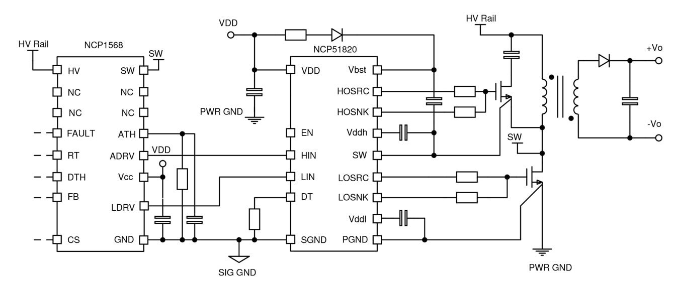
Active Clamp Flyback Application Example
Figure 2: GaN based active clamp flyback converter outline
In Figure 2, an ON Semiconductor NCP51820 GaN gate driver is shown with a NCP1568 active clamp flyback controller. The driver features gate drivers with regulated +5.2V amplitude for high and low side output optimum for controlling E-mode GaN. It also has -3.5V to +650V high-side common-mode voltage range with -3.5 to +3.5V for the low side and 200V/ns immunity, enabled by an innovative junction-insulation technology. Having level shifting for the low-side drive makes Kelvin connection easier if there is a current sense resistor in the low-side device source. Driver waveform rise and fall times are 1ns and maximum propagation delay is 50ns. Separate source and sink outputs are provided so turn-on and turn-off edge rates can be individually controlled for best EMI/efficiency.
LLC Converter Application Example
A feature of the LLC converter (Figure 3) is that drive waveforms are each 50 percent duty cycle. It’s vital therefore that dead time is controlled so no overlap occurs.
Figure 3: GaN based LLC converter outline
The ON Semiconductor NCP51820 driver guarantees that the gate drives cannot overlap. It also includes an enable input and comprehensive protection against supply under-voltage and over-temperature. It is available in a PQFN, 4 x 4mm 15-lead package enabling short, low inductance connections to the GaN device gate.
Board Layout is Critical
In all applications, the board layout is critical for success. The gate driver loops should be minimized and matched, the driver and GaN device should be on the same side of the PCB and ground/power planes used.
GaN switches need a careful design of their gate drive circuit to achieve the promised gains in efficiency and power density with operational reliability. Along with careful layout, a dedicated driver such as the ON Semiconductor NCP51820 with its host of features for high and low-side drives ensures that the GaN devices perform to their best.
Learn more about our NCP51820 high-speed gate driver today!